Caption:
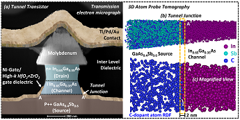
(a) Cross-section micrograph of Tunnel Field-Effect-Transistor (TFET). TFETs are high impact next generation transistors which can provide high performance with extreme energy efficiency compared to conventional silicon-transistors. This high performance stems from quantum mechanical tunneling of electrons across the tunnel junction interface detailed in (b) and (c). TFET fabrication and Transmission Electron Micrograph by Rahul Pandey. Atom Probe characterization of TFET tunnel junction done in collaboration with Markus Kuhn at Intel Corporation (Metrology Group, Hillsboro, OR).
Rahul Pandey
Advisor: Dr. Suman Datta, EE, Pennsylvania State University and University of Notre Dame Department of Electrical Engineering
Pennsylvania State University, University Park, PA 16802
Laboratory website: http://www.ndcl.ee.psu.edu/
Technique: Cross-section micrograph of fabricated III-V compound semiconductor based TFET (Fig. a) is obtained through Transmission Electron Microscopy (TEM). The team at Penn State collaborated with researchers from Intel Corporation to use Atom Probe Tomography and Time-of-flight Spectroscopy to characterize critical tunnel junction interface in TFET (Fig. b and c).
Description:
As we venture into the era of Internet of Things with more intelligent and connected electronic devices, there is an increasing need for more energy efficient data processing. Conventional Silicon-MOS Field-Effect-Transistors (MOSFETs) cannot meet these demands. We are developing a Tunnel Field-Effect-Transistor (TFET) based on III-V arsenide-antimonide hetero-junctions to provide high performance at extremely low power consumption. In a TFET, the electrons undergo quantum mechanical tunneling from the source to the channel region which filters out the high-energy carriers resulting in very steep switching and energy savings. Using III-V arsenide-antimonide hetero-junctions in designing TFETs ensures high performance through high on-current even at extremely low voltages (<0.5 V). Critical to TFET performance when they are made from combinations of III-V materials is the need for abrupt and uniform interfaces among the dissimilar materials. Variability at these interfaces, or heterojunctions, dramatically impacts device performance. It is hence of significant importance to characterize hetero-junction TFETs with precision in nanometer-scale devices which have been presented in the figures.
Funding Source: This work was supported by the National Science Foundation ASSIST Nanosystems ERC under Award Number EEC-1160483.


