How do scientists see what’s going on in the extremely small world of nanotechnology? The microscopes that are typically used in high school and college won’t do the job. Nanoscientists use high-powered microscopes that use unique methods to allow them to see the surface features on the atomic scale, effectively opening the door to modern nanotechnology.
Exploring the World through Microscopes
Beginning as early as the 1930s, scientists were able to see at the nanoscale using instruments such as the scanning electron microscope, the transmission electron microscope, and the field ion microscope. The most recent and notable developments in microscopy are the scanning tunneling microscope and the atomic force microscope.
The electron microscope, first developed by German engineers Ernst Ruska and Max Knoll in the 1930s, uses a particle beam of electrons to illuminate a specimen and create a highly magnified image. Electron microscopes yield much greater resolution than the older light microscopes; they can obtain magnifications of up to 1 million times, while the best light microscopes can magnify an image only about 1,500 times.
 |
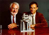
The scanning tunneling microscope (STM) is among a number of instruments that allows scientists to view and manipulate nanoscale particles, atoms, and small molecules. Its development earned its inventors, Gerd Binig and Heinrich Rohrer, the Nobel Prize in Physics in 1986.
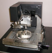
Atomic force microscopes (AFMs) gather information by "feeling" the surface with a mechanical probe. Gerd Binig, along with Calvin Quate and Christoph Gerber, developed the first AFM in 1986.
 |
Atomic Force Microscope |
These microscopes make use of tiny but exact movements to enable precise mechanical scanning.
Additional Microscopy Information
- How the optical microscope became a nanoscope, The Nobel Prize in Chemistry 2014, The Royal Swedish Academy of Sciences
- Molecular Expressions—Science, Optics and You, Florida State University
- Nanoworld Center for Microscopy and Microanalysis, University of Queensland, Australia


